Spin polarized scanning tunneling microscopy
Spin-polarized scanning tunneling microscopy (SP-STM) is a type of scanning tunneling microscope (STM) that can provide detailed information of magnetic phenomena on the single-atom scale additional to the atomic topography gained with STM. SP-STM opened a novel approach to static and dynamic magnetic processes as precise investigations of domain walls in ferromagnetic and antiferromagnetic systems, as well as thermal and current-induced switching of nanomagnetic particles.
Principle of operation
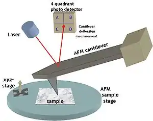
An extremely sharp tip coated with a thin layer of magnetic material is moved systematically over a sample. A voltage is applied between the tip and the sample allowing electrons to tunnel between the two, resulting in a current. In the absence of magnetic phenomena, the strength of this current is indicative for local electronic properties.
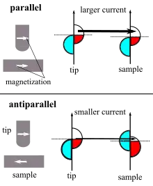
If the tip is magnetized, electrons with spins matching the tip's magnetization will have a higher chance of tunneling. This is essentially the effect of tunnel magnetoresistance and the tip/surface essentially acts as a spin valve.
Since a scan using only a magnetized tip cannot distinguish between current changes due to magnetization or space separation, multi-domain structures and/or topographical information from another source (frequently conventional STM) must be utilized. This makes possible magnetic imaging down to the atomic scale, for example, in antiferromagnetic system. Topographical and magnetic information can be simultaneously obtained if the tip's magnetization is modulated at a high frequency (20–30 kHz) using a small coil wound around the tip. The tip's magnetization thus flips too fast for the STM feedback loop to respond to and topographical information is obtained intact. The high frequency signal is separated using a lock-in amplifier and this signal provides the magnetic information about the surface.
In standard scanning tunneling microscopy (STM), the tunneling probability of electrons between the probe tip and the sample strongly depends on the distance between them, as it decays exponentially as the separation increases. In spin-polarized STM (SP-STM) the tunneling current also depends on the spin-orientation of the tip and the sample. The local density of states (LDOS) of the magnetic tip and the sample is different for different spin orientations, and tunneling can occur only between the states with parallel spin (ignoring spin flip processes). When the spin of sample and the tip are parallel there are many available states to which the electrons can tunnel, thus resulting in a large tunneling current. On the other hand, if the spins are antiparallel most of the available states are already filled and the tunneling current will be significantly smaller. With SP -STM it is then possible to probe the spin dependent local density of states of magnetic samples by measuring the tunneling conductance , which for small bias is given by[1]
where is the tunneling conductance in nonmagnetic case, is the tunneling matrix element which describes the transitions between the spin dependent states of the tip and the sample, , , and , are the total densities of state and polarizations for the tip (t) and the sample (s), respectively, and is the angle between the magnetization directions of the tip and the sample. In the nonmagnetic limit ( or ), this expression reduces to the Tersoff and Hamann model for standard STM tunneling conductance.[1] In the more general case, with finite bias voltage , the expression for the tunneling current at tip location becomes
where is constant, the inverse decay length of the electron wavefunction, and, and the charge and mass of electron, respectively, is the energy-integrated LDOS of the tip, and , and are the corresponding magnetization vectors of the spin-polarized LDOS. The tunneling current is sum of spin-independent , and spin-dependent parts.[2]

Probe tip preparation
The most critical component in the SP-STM setup is the probe tip which has to be atomically sharp to offer spatial resolution down to atomic level, have large enough spin polarization to provide sufficient signal to noise ratio, but at the same time have small enough stray magnetic field to enable nondestructive magnetic probing of the sample, and finally the spin orientation at the tip apex has to be controlled in order to determine which spin orientation of the sample is imaged. In order to prevent oxidization the tip preparation usually has to be done in ultra-high vacuum (UHV). There are three main ways to obtain probe tip suitable for SP-STM measurements:
- Bulk magnetic material (e.g. iron) is first electrochemically etched to form a constriction, and as the material is pulled apart it breaks at the constriction forming a sharp tip. Alternatively, the material can be etched until the tip is formed, but then a tip cleaning procedure in UHV is required. Iron has high saturation magnetization which results in a larger stray field around the tip meaning that nondestructive imaging is not possible. Iron tips can be used to measure antiferromagnetic or ferrimagnetic samples. Amorphous alloys such as have lower saturation magnetization but still nonvanishing stray fields. For nondestructive imaging the tips can be made from antiferromagnetic materials such as or , in this case however, the spin contrast of the imaging is sacrificed due to tunneling currents from to different spin states partially canceling out each other.[3][4]
- Nonmagnetic tip with ultrathin film of magnetic material. Nonmagnetic material is first etched and cleaned with electron bombardment and high temperature flash to remove oxides and other contaminations. The tip is then covered with thin (less than diameter of the tip) layer of magnetic material. In such thin films the magnetization direction is determined by surface and interface anisotropies. Choosing a suitable film material and thickness the tip can be prepared to probe either in-plane or out-of-plane magnetic directions. For ferromagnetic thin films, external magnetic field can be used to tip the magnetization enabling the setup to measure both directions with the same tip. To increase spatial resolution, bias voltage between the tip and the sample can be applied which causes thin film atoms to migrate towards the tip apex making it sharper. Even with thin film deposition, the tip will still carry a magnetic stray field that can perturb the sample.[5][6]
- Nonmagnetic tip with a cluster of magnetic material. In this method voltage pulses are applied between nonmagnetic tip and magnetic sample which causes magnetic material of the sample to attach to the tip. Magnetization direction can be altered by applying further voltage pulses. Alternatively, the tip can be dipped in the magnetic material and then retracted leaving a cluster attached to the tip assuming that the magnetic material properly wets the tip. The tip size is not controlled as in ultrathin film deposition.[7][8]
Modes of Operation
SP-STM can be operated in one of three modes: constant current, and spectroscopic mode which are similar to standard STM operation modes but with spin-resolution, or modulated tip magnetization mode which is unique to SP-STM measurements. In constant current mode, the tip-sample separation is kept constant by an electric feedback loop. The measured tunneling current consists of spin-averaged and spin-dependent components () which can be decomposed from the data. Tunneling current is primarily dominated by the smallest non-zero reciprocal lattice vector, which means that as magnetic superstructures usually have the longest real space periodicities (and thus the shortest reciprocal space periodicities), bring the largest contribution to the spin-dependent tunneling current . Thus SP-STM is an excellent method to observe magnetic structure rather than atomic structure of the sample. The downside is that it is difficult to study larger than atomic scales in constant-current mode as the topographical features of the surface may interfere with the magnetic features making data analysis very difficult.[9][1]
The second mode of operation is spin-resolved spectroscopic mode which measures local differential tunneling conductance as a function of bias voltage and spatial coordinates of the tip. Spectroscopic mode can be used under constant-current conditions in which the sample-tip separation varies resulting in superposition of topographic and electronic information which can then be separated. If spectroscopic mode is used with constant tip-sample separation, the measured is directly related to the spin-resolved LDOS of the sample whereas the measured tunneling current is proportional to the energy-integrated spin-polarized LDOS. By combining the spectroscopic mode with constant-current mode, it is possible to obtain both topographic and spin-resolved surface data.[1]
Thirdly, SP-STM can be used in modulated magnetization mode in which the tip magnetization is periodically switched resulting in a tunneling current that is proportional to the local magnetization of the sample. This enables it to separate magnetic features from electronic and topographical features. Since spin-polarized LDOS can change not only magnitude but also sign as a function of energy, the measured tunneling current can vanish even if there is finite magnetization in the sample. Thus bias dependence of the spin-polarized tunneling current in modulated magnetization mode has to be studied as well. Only ferromagnetic tips are suitable for modulated magnetization mode meaning that their stray fields might make nondestructive imaging impossible.[10]
Applications of SP-STM
The spin polarized scanning tunneling microscope is a versatile instrument which has gained tremendous attention due to its enhanced surface sensitivity and lateral resolution up to atomic scale, and can be used as an important tool to study ferromagnetic materials, such as Dysprosium (Dy), quasi-2D thin films, nano islands and quasi-1D nanowire that have high magnetic anisotropy, etc. In a study carried out by L. Berbil-Bautista et al.,[11] the magnetic domain wall or Néel wall of the width 2-5 nm present in these materials is observed by bringing the Chromium (Cr) coated Tungsten tip close to the Dy layer. This causes the transfer of Dy particles from magnetic material on to the apex of the tip. The width of the domain wall is calculated as
where is exchange stiffness. The magnetic contrast is enhanced due to the presence of electronic states that are not occupied in the cluster of Dy atoms present on the apex of the tip.[11]

The formation of 360° domain walls in ferromagnetic films plays an important role in making magnetic random access memory devices. These domain walls are formed when an external magnetic field is applied along the easy direction of magnetic material. This forces the two 180° walls, which also have identical sense of rotation to come closer. In a study carried out by A. Kubetzka et al.,[12] the SP-STM was used to measure the evolution of 360° domain wall profiles of two atomic layer iron nanowires by varying the external magnetic field between 550-800 mT.[12]
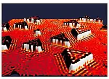
The quantum interference phenomena has been observed in Cobalt islands deposited on Copper(111) substrate. This has been attributed to the fact that scattering caused by surface state electron defects, such as terrace edges, impurities or adsorbates present on a densely packed noble metal surface. Spin polarized-STM has been used to investigate the electronic structure of triangular Cobalt islands deposited on Copper(111). This study shows that the substrate and islands exhibit their individual standing wave patterns and this can be used to find the spin polarized material.[13]
New advances in SP-STM

New advances in SP-STM shows that this technique can be further used to understand complex phenomena that have not been explained by other imaging techniques. Non-magnetic impurities, such as oxygen on magnetic surface (Iron double layer on Tungsten (W) substrate) causes formation of spin polarized waves. The adsorbed oxygen impurity on iron double layer can be used to study the interaction between Kondo impurties on RKKY inteaction. This study shows that anisotropic scattering states can be observed around individual oxygen atoms adsorbed on iron double layer. This gives information on spin characteristics of electronic states involved in the scattering process.[14]
Similarly, existence of 2D anti-ferromagnetism at the interface of Manganese (Mn) and W(110) has been observed using SP-STM technique. The importance of this study is that the atomic scale roughness at the interface between Mn and W(110) causes frustration in magnetic interaction, and it gives rise to complex spin structures that cannot be studied using other methods.[15]
Alternate method
Another way to obtain the magnetization distribution is to have the tip provide a strong stream of spin polarized electrons. One method to achieve this is to shine polarization laser light onto a GaAs tip, which produces spin polarized electrons due to spin-orbit coupling. The tip is then scanned along the sample much like conventional STM .[16] One limitation of this method is that the most effective source of spin polarized electrons is obtained by having the incident laser light shine directly opposite of the tip, i.e. through the sample itself. This restricts the method to measuring thin samples.
See also
References
- Wiesendanger, Roland (2009-11-18). "Spin mapping at the nanoscale and atomic scale". Reviews of Modern Physics. 81 (4): 1495–1550. Bibcode:2009RvMP...81.1495W. doi:10.1103/RevModPhys.81.1495.
- Wortmann, D.; Heinze, S.; Kurz, Ph.; Bihlmayer, G.; Blügel, S. (2001-04-30). "Resolving Complex Atomic-Scale Spin Structures by Spin-Polarized Scanning Tunneling Microscopy" (PDF). Physical Review Letters. 86 (18): 4132–4135. Bibcode:2001PhRvL..86.4132W. doi:10.1103/PhysRevLett.86.4132. PMID 11328113.
- Wiesendanger, R.; Bürgler, D.; Tarrach, G.; Schaub, T.; Hartmann, U.; Güntherodt, H.-J.; Shvets, I. V.; Coey, J. M. D. (1991-11-01). "Recent advances in scanning tunneling microscopy involving magnetic probes and samples". Applied Physics A. 53 (5): 349–355. Bibcode:1991ApPhA..53..349W. doi:10.1007/BF00348147. ISSN 0947-8396.
- Wulfhekel, W; Hertel, R; Ding, H.F; Steierl, G; Kirschner, J (2002). "Amorphous, low magnetostriction tips for spin-polarized scanning tunneling microscopy". Journal of Magnetism and Magnetic Materials. 249 (1–2): 368–374. Bibcode:2002JMMM..249..368W. doi:10.1016/s0304-8853(02)00560-7. ISSN 0304-8853.
- Bode, M.; Pascal, R. (1997). "Scanning tunneling spectroscopy of Fe/W(110) using iron covered probe tips". Journal of Vacuum Science & Technology A. 15 (3): 1285–1290. Bibcode:1997JVSTA..15.1285B. doi:10.1116/1.580577.
- Getzlaff, M.; Bode, M.; Heinze, S.; Pascal, R.; Wiesendanger, R. (1998). "Temperature-dependent exchange splitting of the magnetic Gd(0001) surface state". Journal of Magnetism and Magnetic Materials. 184 (2): 155–165. Bibcode:1998JMMM..184..155G. doi:10.1016/s0304-8853(97)01140-2. ISSN 0304-8853.
- Yamada, T. K. (2003). "Use of voltage pulses to detect spin-polarized tunneling". Appl. Phys. Lett. 82 (9): 1437–1439. Bibcode:2003ApPhL..82.1437Y. doi:10.1063/1.1556958.
- Binnig, Gerd (1987). "Scanning tunneling microscopy—from birth to adolescence". Reviews of Modern Physics. 59 (3): 615–625. Bibcode:1987RvMP...59..615B. doi:10.1103/RevModPhys.59.615.
- Binnig, Gerd; Rohrer, Heinrich (1987-07-01). "Scanning tunneling microscopy---from birth to adolescence". Reviews of Modern Physics. 59 (3): 615–625. Bibcode:1987RvMP...59..615B. doi:10.1103/RevModPhys.59.615.
- Wulfhekel, Wulf; Kirschner, Jürgen (1999). "Spin-polarized scanning tunneling microscopy on ferromagnets". Appl. Phys. Lett. 75 (13): 1944. Bibcode:1999ApPhL..75.1944W. doi:10.1063/1.124879.
- Berbil-Bautista, L. (2007). "Spin-polarized scanning tunneling microscopy and spectroscopy of ferromagnetic Dy(0001)/W(110) films". Physical Review B. 76 (6): 064411. Bibcode:2007PhRvB..76f4411B. doi:10.1103/PhysRevB.76.064411.
- Kubetzka, A. (2003). "Spin-polarized scanning tunneling microscopy study of". Physical Review B. 67 (2): 020401. Bibcode:2003PhRvB..67b0401K. doi:10.1103/PhysRevB.67.020401.
- Pietzsch, O. (2006). "Spin-Resolved Electronic Structure of Nanoscale Cobalt Islands on Cu(111)". Physical Review Letters. 96 (23): 237203. Bibcode:2006PhRvL..96w7203P. doi:10.1103/PhysRevLett.96.237203. PMID 16803397.
- von Bergmann, K. (2004). "Spin-Polarized Electron Scattering at Single Oxygen Adsorbates on a Magnetic Surface". Physical Review Letters. 92 (4): 046801. Bibcode:2004PhRvL..92d6801V. doi:10.1103/PhysRevLett.92.046801. PMID 14995391.
- Wortmann, D. (2001). "Resolving Complex Atomic-Scale Spin Structures by Spin-Polarized Scanning Tunneling Microscopy" (PDF). Physical Review Letters. 86 (18): 4132–4135. Bibcode:2001PhRvL..86.4132W. doi:10.1103/PhysRevLett.86.4132. PMID 11328113.
- Laiho, R.; Reittu, H. (1993). "Theory of scanning tunneling microscopy with spin-polarized electrons obtained from a semiconducting tip". Surface Science. 289 (3). doi:10.1016/0039-6028(93)90667-9.
External links
- A brief overview of STM
- Bode, M (2003). "Spin-polarized scanning tunnelling microscopy". Reports on Progress in Physics. 66 (4): 523–582. Bibcode:2003RPPh...66..523B. doi:10.1088/0034-4885/66/4/203.
