Scanning Hall probe microscope
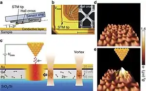
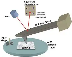
Scanning Hall probe microscope (SHPM) is a variety of a scanning probe microscope which incorporates accurate sample approach and positioning of the scanning tunnelling microscope with a semiconductor Hall sensor. This combination allows mapping the magnetic induction associated with a sample. Current state of the art SHPM systems utilize 2D electron gas materials (e.g. GaAs/AlGaAs) to provide high spatial resolution (~300 nm) imaging with high magnetic field sensitivity. Unlike the magnetic force microscope the SHPM provides direct quantitative information on the magnetic state of a material. The SHPM can also image magnetic induction under applied fields up to ~1 tesla and over a wide range of temperatures (millikelvins to 300 K).[2]

The SHPM can be used to image many types of magnetic structures such as thin films, permanent magnets, MEMS structures, current carrying traces on PCBs, permalloy disks, and recording media
Advantages to other magnetic raster scanning methods
SHPM is a superior magnetic imaging technique due to many reasons. Unlike the MFM technique, the Hall probe exerts negligible force on the underlying magnetic structure and is noninvasive. Unlike the magnetic decoration technique, the same area can be scanned over and over again. The magnetic field caused by hall probe is so minimal it has a negligible effect on sample it is measuring. The sample does not need to be an electrical conductor, unless using STM for height control. The measurement can be performed from 5 – 500 K in ultra high vacuum (UHV) and is nondestructive to the crystal lattice or structure. Tests requires no special surface preparation or coating. The detectable magnetic field sensitivity, is approximately 0.1 uT – 10 T. SHPM can be combined with other scanning methods such as STM.
Limitations
There are some shortcomings or difficulties when working with an SHPM. High resolution scans become difficult due to the thermal noise of extremely small hall probes. There is a minimum scanning height distance due to the construction of the hall probe. (This is especially significant with 2DEG semi-conductor probes due to their multi-layer design). The scanning (lift) height affects obtained image. Scanning large areas takes a significant amount of time. There is a relatively short practical scanning range (order of 1000s micrometer) along any direction. The housing is important to shield electromagnetic noise (Faraday cage), acoustic noise (anti-vibrating tables), air flow (air isolation cupboard), and static charge on the sample (ionizing units).
References
- Ge, Jun-Yi; Gladilin, Vladimir N.; Tempere, Jacques; Xue, Cun; Devreese, Jozef T.; Van De Vondel, Joris; Zhou, Youhe; Moshchalkov, Victor V. (2016). "Nanoscale assembly of superconducting vortices with scanning tunnelling microscope tip". Nature Communications. 7: 13880. arXiv:1701.06316. Bibcode:2016NatCo...713880G. doi:10.1038/ncomms13880. PMC 5155158. PMID 27934960.
- Chang, A. M.; Hallen, H. D.; Harriott, L.; Hess, H. F.; Kao, H. L.; Kwo, J.; Miller, R. E.; Wolfe, R.; Van Der Ziel, J.; Chang, T. Y. (1992). "Scanning Hall probe microscopy". Appl. Phys. Lett. 61 (16): 1974. Bibcode:1992ApPhL..61.1974C. doi:10.1063/1.108334.
