Boost converter
A boost converter (step-up converter) is a DC-to-DC power converter that steps up voltage (while stepping down current) from its input (supply) to its output (load). It is a class of switched-mode power supply (SMPS) containing at least two semiconductors (a diode and a transistor) and at least one energy storage element: a capacitor, inductor, or the two in combination. To reduce voltage ripple, filters made of capacitors (sometimes in combination with inductors) are normally added to such a converter's output (load-side filter) and input (supply-side filter).


Overview
Power for the boost converter can come from any suitable DC source, such as batteries, solar panels, rectifiers, and DC generators. A process that changes one DC voltage to a different DC voltage is called DC to DC conversion. A boost converter is a DC to DC converter with an output voltage greater than the source voltage. A boost converter is sometimes called a step-up converter since it "steps up" the source voltage. Since power () must be conserved, the output current is lower than the source current.
History
For high efficiency, the switched-mode power supply (SMPS) switch must turn on and off quickly and have low losses. The advent of a commercial semiconductor switch in the 1950s represented a major milestone that made SMPSs such as the boost converter possible. The major DC to DC converters were developed in the early 1960s when semiconductor switches had become available. The aerospace industry’s need for small, lightweight, and efficient power converters led to the converter’s rapid development.
Switched systems such as SMPS are a challenge to design since their models depend on whether a switch is opened or closed. R. D. Middlebrook from Caltech in 1977 published the models for DC to DC converters used today. Middlebrook averaged the circuit configurations for each switch state in a technique called state-space averaging. This simplification reduced two systems into one. The new model led to insightful design equations which helped the growth of SMPS.
Applications
Battery power systems
Battery power systems often stack cells in series to achieve higher voltage. However, sufficient stacking of cells is not possible in many high voltage applications due to lack of space. Boost converters can increase the voltage and reduce the number of cells. Two battery-powered applications that use boost converters are used in hybrid electric vehicles (HEV) and lighting systems.
The NHW20 model Toyota Prius HEV uses a 500 V motor. Without a boost converter, the Prius would need nearly 417 cells to power the motor. However, a Prius actually uses only 168 cells and boosts the battery voltage from 202 V to 500 V. Boost converters also power devices at smaller scale applications, such as portable lighting systems. A white LED typically requires 3.3 V to emit light, and a boost converter can step up the voltage from a single 1.5 V alkaline cell to power the lamp.
Joule thief
An unregulated boost converter is used as the voltage increase mechanism in the circuit known as the 'Joule thief', based on blocking oscillator concepts. This circuit topology is used with low power battery applications, and is aimed at the ability of a boost converter to 'steal' the remaining energy in a battery. This energy would otherwise be wasted since the low voltage of a nearly depleted battery makes it unusable for a normal load. This energy would otherwise remain untapped because many applications do not allow enough current to flow through a load when voltage decreases. This voltage decrease occurs as batteries become depleted, and is a characteristic of the ubiquitous alkaline battery. Since the equation for power is , and R tends to be stable, power available to the load goes down significantly as voltage decreases.
Photovoltaic cells
The special kind of boost-converters called Voltage-Lift Type Boost Converters are used in solar photovoltaic (PV) systems. These power converters add up the passive components (diode, inductor and capacitor) of a traditional boos-converter to improve the power quality and increase the performance of complete PV system.[1]
Circuit analysis


Operation
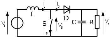
The key principle that drives the boost converter is the tendency of an inductor to resist changes in current by either increasing or decreasing the energy stored in the inductor magnetic field. In a boost converter, the output voltage is always higher than the input voltage. A schematic of a boost power stage is shown in Figure 1.
(a) When the switch is closed, current flows through the inductor in the clockwise direction and the inductor stores some energy by generating a magnetic field. Polarity of the left side of the inductor is positive.

(b) When the switch is opened, current will be reduced as the impedance is higher. The magnetic field previously created will be reduced in energy to maintain the current towards the load. Thus the polarity will be reversed (meaning the left side of the inductor will become negative). As a result, two sources will be in series causing a higher voltage to charge the capacitor through the diode D.
If the switch is cycled fast enough, the inductor will not discharge fully in between charging stages, and the load will always see a voltage greater than that of the input source alone when the switch is opened. Also while the switch is opened, the capacitor in parallel with the load is charged to this combined voltage. When the switch is then closed and the right hand side is shorted out from the left hand side, the capacitor is therefore able to provide the voltage and energy to the load. During this time, the blocking diode prevents the capacitor from discharging through the switch. The switch must of course be opened again fast enough to prevent the capacitor from discharging too much.
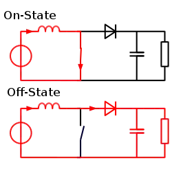
The basic principle of a Boost converter consists of 2 distinct states (see figure 2):
- in the On-state, the switch S (see figure 1) is closed, resulting in an increase in the inductor current;
- in the Off-state, the switch is open and the only path offered to inductor current is through the flyback diode D, the capacitor C and the load R. This results in transferring the energy accumulated during the on-state into the capacitor.
- The input current is the same as the inductor current as can be seen in figure 2. So it is not discontinuous as in the buck converter and the requirements on the input filter are relaxed compared to a buck converter.
Continuous mode
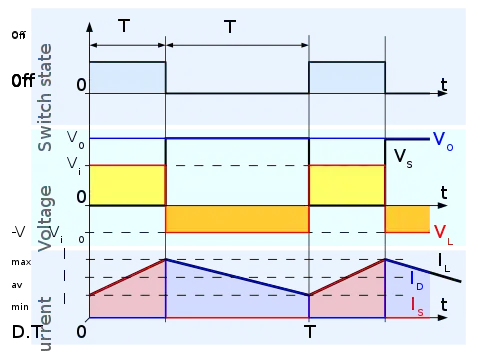
When a boost converter operates in continuous mode, the current through the inductor () never falls to zero. Figure 3 shows the typical waveforms of inductor current and voltage in a converter operating in this mode.

In the steady state, the DC (average) voltage across the inductor must be zero so that after each cycle the inductor returns the same state, because voltage across the inductor is proportional to rate of change of current through it (explained in more detail below). Note in Figure 1 that the left hand side of L is at and the right hand side of L sees the voltage waveform from Figure 3. The average value of is where D is the duty cycle of the waveform driving the switch. From this we get the ideal transfer function:
or
.
We get the same result from a more detailed analysis as follows: The output voltage can be calculated as follows, in the case of an ideal converter (i.e. using components with an ideal behaviour) operating in steady conditions:[2]
During the on-state, the switch S is closed, which makes the input voltage () appear across the inductor, which causes a change in current () flowing through the inductor during a time period (t) by the formula:
Where L is the inductor value.
At the end of the on-state, the increase of IL is therefore:
D is the duty cycle. It represents the fraction of the commutation period T during which the switch is on. Therefore, D ranges between 0 (S is never on) and 1 (S is always on).
During the Off-state, the switch S is open, so the inductor current flows through the load. If we consider zero voltage drop in the diode, and a capacitor large enough for its voltage to remain constant, the evolution of IL is:
Therefore, the variation of IL during the Off-period is:
As we consider that the converter operates in steady state conditions, the amount of energy stored in each of its components has to be the same at the beginning and at the end of a commutation cycle. In particular, the energy stored in the inductor is given by:
So, the inductor current has to be the same at the start and end of the commutation cycle. This means the overall change in the current (the sum of the changes) is zero:
Substituting and by their expressions yields:
This can be written as:
The above equation shows that the output voltage is always higher than the input voltage (as the duty cycle goes from 0 to 1), and that it increases with D, theoretically to infinity as D approaches 1. This is why this converter is sometimes referred to as a step-up converter.
Rearranging the equation reveals the duty cycle to be:
Discontinuous mode
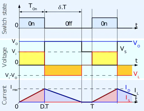
If the ripple amplitude of the current is too high, the inductor may be completely discharged before the end of a whole commutation cycle. This commonly occurs under light loads. In this case, the current through the inductor falls to zero during part of the period (see waveforms in figure 4). Although the difference is slight, it has a strong effect on the output voltage equation.

The voltage gain can be calculated as follows:
As the inductor current at the beginning of the cycle is zero, its maximum value (at ) is
During the off-period, IL falls to zero after :
Using the two previous equations, δ is:
The load current Io is equal to the average diode current (ID). As can be seen on figure 4, the diode current is equal to the inductor current during the off-state. The average value of Io can be sorted out geometrically from figure 4. Therefore, the output current can be written as:
Replacing ILmax and δ by their respective expressions yields:
Therefore, the output voltage gain can be written as follows:
Compared to the expression of the output voltage gain for continuous mode, this expression is much more complicated. Furthermore, in discontinuous operation, the output voltage gain not only depends on the duty cycle (D), but also on the inductor value (L), the input voltage (Vi), the commutation period (T) and the output current (Io).
Substituting into the equation (R is the load), the output voltage gain can be rewritten as:
where
See also
- Joule thief
- Buck converter
- Buck-boost converter
- Split-pi topology
- Transformer
- Vibrator (electronic)
- Voltage doubler
- Voltage multiplier
- The hydraulic ram can be seen as analogous to a boost converter, using the electronic–hydraulic analogy.[4][5]
Further reading
References
- Sharma, Kalyani; B., Raj Kiran (November 2016). "Simulation Analysis of Voltage-Lift Type Boost Converter for Solar Photovoltaic System". International Journal of Science and Research. 5 (11): 1899–1903 – via IJSR.
- "Boost Converter Operation". LT1070 Design Manual, Carl Nelson & Jim Williams
- Kypuros, Javier A.; Longoria, Raul G. (2004-01-29). "Model Synthesis for Design of Switched Systems Using a Variable Structure System Formulation". Journal of Dynamic Systems, Measurement, and Control. 125 (4): 618–629. doi:10.1115/1.1636774. ISSN 0022-0434.
The hydraulic-ram pump ... structure parallels that of the boost converter making it a hydraulic analog
- Longoria, R.G.; Kypuros, J.A.; Raynter, H.M. (1997). "Bond graph and wave-scattering models of switched power conversion". 1997 IEEE International Conference on Systems, Man, and Cybernetics. Computational Cybernetics and Simulation. 2. pp. 1522–1526. doi:10.1109/ICSMC.1997.638209. ISBN 978-0-7803-4053-4.
Indeed, this self-acting pump has much to offer in a parallel study with its electrical cousin.
External links
| Wikimedia Commons has media related to Boost converters. |