Staggered tuning
Staggered tuning is a technique used in the design of multi-stage tuned amplifiers whereby each stage is tuned to a slightly different frequency. In comparison to synchronous tuning (where each stage is tuned identically) it produces a wider bandwidth at the expense of reduced gain. It also produces a sharper transition from the passband to the stopband. Both staggered tuning and synchronous tuning circuits are easier to tune and manufacture than many other filter types.
The function of stagger-tuned circuits can be expressed as a rational function and hence they can be designed to any of the major filter responses such as Butterworth and Chebyshev. The poles of the circuit are easy to manipulate to achieve the desired response because of the amplifier buffering between stages.
Applications include television IF amplifiers (mostly 20th century receivers) and wireless LAN.
Rationale
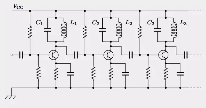
Staggered tuning improves the bandwidth of a multi-stage tuned amplifier at the expense of the overall gain. Staggered tuning also increases the steepness of passband skirts and hence improves selectivity.[1]
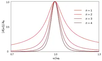
The value of staggered tuning is best explained by first looking at the shortcomings of tuning every stage identically. This method is called synchronous tuning. Each stage of the amplifier will reduce the bandwidth. In an amplifier with multiple identical stages, the 3 dB points of the response after the first stage will become the 6 dB points of the second stage. Each successive stage will add a further 3 dB to what was the band edge of the first stage. Thus the 3 dB bandwidth becomes progressively narrower with each additional stage.[2]
As an example, a four-stage amplifier will have its 3 dB points at the 0.75 dB points of an individual stage. The fractional bandwidth of an LC circuit is given by,
- where m is the power ratio of the power at resonance to that at the band edge frequency (equal to 2 for the 3 dB point and 1.19 for the 0.75 dB point) and Q is the quality factor.
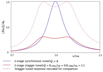
The bandwidth is thus reduced by a factor of . In terms of the number of stages .[3] Thus, the four stage synchronously tuned amplifier will have a bandwidth of only 19% of a single stage. Even in a two-stage amplifier the bandwidth is reduced to 41% of the original. Staggered tuning allows the bandwidth to be widened at the expense of overall gain. The overall gain is reduced because when any one stage is at resonance (and thus maximum gain) the others are not, unlike synchronous tuning where all stages are at maximum gain at the same frequency. A two-stage stagger-tuned amplifier will have a gain 3 dB less than a synchronously tuned amplifier.[4]
Even in a design that is intended to be synchronously tuned, some staggered tuning effect is inevitable because of the practical impossibility of keeping all tuned circuits perfectly in step and because of feedback effects. This can be a problem in very narrow band applications where essentially only one spot frequency is of interest, such as a local oscillator feed or a wave trap. The overall gain of a synchronously tuned amplifier will always be less than the theoretical maximum because of this.[5]
Both synchronously tuned and stagger-tuned schemes have a number of advantages over schemes that place all the tuning components in a single aggregated filter circuit separate from the amplifier such as ladder networks or coupled resonators. One advantage is that they are easy to tune. Each resonator is buffered from the others by the amplifier stages so have little effect on each other. The resonators in aggregated circuits, on the other hand, will all interact with each other, particularly their nearest neighbours.[6] Another advantage is that the components need not be close to ideal. Every LC resonator is directly working into a resistor which lowers the Q anyway so any losses in the L and C components can be absorbed into this resistor in the design. Aggregated designs usually require high Q resonators. Also, stagger-tuned circuits have resonator components with values that are quite close to each other and in synchronously tuned circuits they can be identical. The spread of component values is thus less in stagger-tuned circuits than in aggregated circuits.[7]
Design
Tuned amplifiers such as the one illustrated at the beginning of this article can be more generically depicted as a chain of transconductance amplifiers each loaded with a tuned circuit.

- where for each stage (omitting the suffixes)
- gm is the amplifier transconductance
- C is the tuned circuit capacitance
- L is the tuned circuit inductance
- G is the sum of the amplifier output conductance and the input conductance of the next amplifier.
Stage gain
The gain A(s), of one stage of this amplifier is given by;
- where s is the complex frequency operator.
This can be written in a more generic form, that is, not assuming that the resonators are the LC type, with the following substitutions,
- (the resonant frequency)
- (the gain at resonance)
- (the stage quality factor)
Resulting in,
Stage bandwidth
The gain expression can be given as a function of (angular) frequency by making the substitution s = iω where i is the imaginary unit and ω is the angular frequency
The frequency at the band edges, ωc, can be found from this expression by equating the value of the gain at the band edge to the magnitude of the expression,
- where m is defined as above and equal to two if the 3 dB points are desired.
Solving this for ωc and taking the difference between the two positive solutions finds the bandwidth Δω,
and the fractional bandwidth B,
Overall response
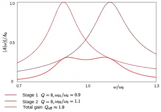
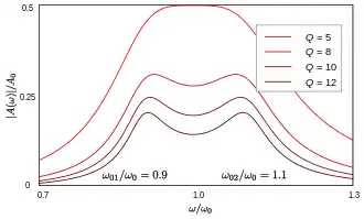
The overall response of the amplifier is given by the product of the individual stages,
It is desirable to be able to design the filter from a standard low-pass prototype filter of the required specification. Frequently, a smooth Butterworth response will be chosen[8] but other polynomial functions can be used that allow ripple in the response.[9] A popular choice for a polynomial with ripple is the Chebyshev response for its steep skirt.[10] For the purpose of transformation, the stage gain expression can be rewritten in the more suggestive form,
This can be transformed into a low-pass prototype filter with the transform
- where ω'c is the cutoff frequency of the low-pass prototype.
This can be done straightforwardly for the complete filter in the case of synchronously tuned amplifiers where every stage has the same ω0 but for a stagger-tuned amplifier there is no simple analytical solution to the transform. Stagger-tuned designs can be approached instead by calculating the poles of a low-pass prototype of the desired form (e.g. Butterworth) and then transforming those poles to a band-pass response. The poles so calculated can then be used to define the tuned circuits of the individual stages.
Poles
The stage gain can be rewritten in terms of the poles by factorising the denominator;
- where p, p* are a complex conjugate pair of poles
and the overall response is,
- where the ak = A0kω0k/Q0k
From the band-pass to low-pass transform given above, an expression can be found for the poles in terms of the poles of the low-pass prototype, qk,
- where ω0B is the desired band-pass centre frequency and Qeff is the effective Q of the overall circuit.
Each pole in the prototype transforms to a complex conjugate pair of poles in the band-pass and corresponds to one stage of the amplifier. This expression is greatly simplified if the cutoff frequency of the prototype, ω'c, is set to the final filter bandwidth ω0B/Qeff.
In the case of a narrowband design ω0≫q which can be used to make a further simplification with the approximation,
These poles can be inserted into the stage gain expression in terms of poles. By comparing with the stage gain expression in terms of component values, those component values can then be calculated.[11]
Applications
Staggered tuning is of most benefit in wideband applications. It was formerly commonly used in television receiver IF amplifiers. However, SAW filters are more likely to be used in that role nowadays.[12] Staggered tuning has advantages in VLSI for radio applications such as wireless LAN.[13] The low spread of component values make it much easier to implement in integrated circuits than traditional ladder networks.[14]
See also
References
- Pederson & Mayaram, p. 259
- Sedha, p. 627
- Chattopadhyay, p. 195
- Maheswari & Anand, p. 500
- Pederson & Mayaram, p. 259
- Iniewski, pp. 200-201
- Wiser, pp. 47-48
- Sedha, p. 627
- Moxon, pp. 88-89
- Iniewski, p. 200
- Maheswari & Anand, pp. 499-500
- Gulati, p. 147
- Wiser, p. vi
- Iniewski, p. 200
Bibliography
- Chattopadhyay, D., Electronics: Fundamentals and Applications, New Age International, 2006 ISBN 8122417809.
- Gulati, R. R., Modern Television Practice Principles,Technology and Servicing, New Age International, 2002 ISBN 8122413609.
- Iniewski, Krzysztof, CMOS Nanoelectronics: Analog and RF VLSI Circuits, McGraw Hill Professional, 2011 ISBN 0071755667.
- Maheswari, L. K.; Anand, M. M. S., Analog Electronics, PHI Learning, 2009 ISBN 8120327225.
- Moxon, L. A., Recent Advances in Radio Receivers, Cambridge University Press, 1949 OCLC 2434545.
- Pederson, Donald O.; Mayaram, Kartikeya, Analog Integrated Circuits for Communication, Springer, 2007 ISBN 0387680292.
- Sedha, R. S., A Textbook of Electronic Circuits, S. Chand, 2008 ISBN 8121928036.
- Wiser, Robert, Tunable Bandpass RF Filters for CMOS Wireless Transmitters, ProQuest, 2008 ISBN 0549850570.