Intel 8255
The Intel 8255 (or i8255) Programmable Peripheral Interface (PPI) chip was developed and manufactured by Intel in the first half of the 1970s for the Intel 8080 microprocessor. The 8255 provides 24 parallel input/output lines with a variety of programmable operating modes.


The 8255 is a member of the MCS-85 Family of chips, designed by Intel for use with their 8085 and 8086 microprocessors and their descendants.[1] It was first available in a 40-pin DIP and later a 44-pin PLCC packages.[2] It found wide applicability in digital processing systems and was later cloned by other manufacturers. The 82C55 is a CMOS version for higher speed and lower current consumption.
The functionality of the 8255 is now mostly embedded in larger VLSI processing chips as a sub-function. A CMOS version of the 8255 is still being made[3] by Renesas but mostly used to expand the I/O of microcontrollers.
Similar chips
The 8255 has a similar function to the MOS Technology 6522 (Versatile Interface Adapter) and the 6526 MOS Technology CIA (Complex Interface Adapter), both developed for the 6502 family.
All of these chips were originally available in a 40-pin DIL package. The 8255 provides 24 usable I/O pins whereas the MOS chips only provide 16 I/O pins plus 4 control pins. However, the MOS chips contain more functions, such as two programmable reload timers and a simple I/O shift register function. Furthermore, the MOS devices allow the direction (input or output) of all their I/O pins to be individually programmed. The 8255 I/O pins have only four programmable direction bits: one for all of Port A(7:0), one for Port B(7:0), one for Port C(3:0) and one for Port C(7:4).
Other comparable microprocessor I/O chips are the 2655 Programmable Peripheral Interface from the Signetics 2650 family, the Motorola 6820 PIA (Peripheral Interface Adapter) from the Motorola 6800 family and the Western Design Center WDC 65C21.
Applications
The 8255 was widely used in many microcomputer/microcontroller systems and home computers such as the SV-328 and all MSX models. The 8255 was used in the original IBM-PC,[6] PC/XT, PC/jr and clones, along with numerous homebuilt computers such as the N8VEM.
Function
The 8255 gives a CPU or digital system access to programmable parallel I/O.[7] The 8255 has 24 input/output pins.[8] These are divided into three 8-bit ports (A, B, C).[9] Port A and port B can be used as 8-bit input/output ports. Port C can be used as an 8-bit input/output port or as two 4-bit input/output ports or to produce handshake signals for ports A and B.
The three ports are further grouped as follows:
- Group A consisting of port A and upper part of port C.
- Group B consisting of port B and lower part of port C.
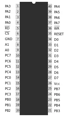
Eight data lines (D0–D7) are available (with an 8-bit data buffer) to read/write data into the ports or control register under the status of the RD (pin 5) and WR (pin 36), which are active-low signals for read and write operations respectively. Address lines A1 and A0 allow to access a data register for each port or a control register, as listed below:
A1 A0 Port selected 0 0 port A 0 1 port B 1 0 port C 1 1 control register
The control signal chip select CS (pin 6) is used to enable the 8255 chip. It is an active-low signal, i.e., when CS = 0, the 8255 is enabled. The RESET input (pin 35) is connected to the RESET line of system like 8085, 8086, etc., so that when the system is reset, all the ports are initialized as input lines. This is done to prevent 8255 and/or any peripheral connected to it from being destroyed due to mismatch of ports. As an example, consider an input device connected to 8255 at port A. If from the previous operation, port A is initialized as an output port and if 8255 is not reset before using the current configuration, then there is a possibility of damage of either the input device connected or 8255 or both, since both 8255 and the device connected will be sending out data.
The control register (or the control logic, or the command word register) is an 8-bit register used to select the modes of operation and input/output designation of the ports.[10]
Operational modes of 8255
There are two basic operational modes of 8255:
- Bit Set/Reset mode (BSR mode).
- Input/Output mode (I/O mode).
The two modes are selected on the basis of the value present at the D7 bit of the control word register. When D7 = 1, 8255 operates in I/O mode, and when D7 = 0, it operates in the BSR mode.
Bit Set/Reset (BSR) mode
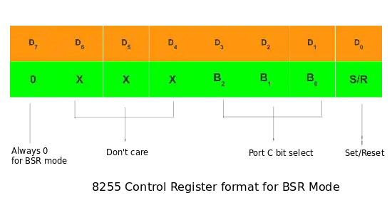
The Bit Set/Reset (BSR) mode is available on port C only. Each line of port C (PC7 - PC0) can be set or reset by writing a suitable value to the control word register. BSR mode and I/O mode are independent and selection of BSR mode does not affect the operation of other ports in I/O mode.[11]

- D7 bit is always 0 for BSR mode.
- Bits D6, D5 and D4 are don't care bits.
- Bits D3, D2 and D1 are used to select the pin of Port C.
- Bit D0 is used to set/reset the selected pin of Port C.
Selection of port C pin is determined as follows:
| D3 | D2 | D1 | Bit/pin of port C selected |
|---|---|---|---|
| 0 | 0 | 0 | PC0 |
| 0 | 0 | 1 | PC1 |
| 0 | 1 | 0 | PC2 |
| 0 | 1 | 1 | PC3 |
| 1 | 0 | 0 | PC4 |
| 1 | 0 | 1 | PC5 |
| 1 | 1 | 0 | PC6 |
| 1 | 1 | 1 | PC7 |
As an example, if it is needed that PC5 be set, then in the control word,
- Since it is BSR mode, D7 = '0'.
- Since D4, D5, D6 are not used, assume them to be '0'.
- PC5 has to be selected, hence, D3 = '1', D2 = '0', D1 = '1'.
- PC5 has to be set, hence, D0 = '1'.
Thus, as per the above values, 0B (Hex) will be loaded into the Control Word Register (CWR).
| D7 | D6 | D5 | D4 | D3 | D2 | D1 | D0 |
|---|---|---|---|---|---|---|---|
| 0 | 0 | 0 | 0 | 1 | 0 | 1 | 1 |
Input/Output mode
This mode is selected when D7 bit of the Control Word Register is 1. There are three I/O modes:[12]
- Mode 0 - Simple I/O
- Mode 1 - Strobed I/O
- Mode 2 - Strobed Bi-directional I/O
Control Word format

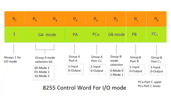
- D0, D1, D3, D4 are assigned for port C lower, port B, port C upper and port A respectively. When these bits are 1, the corresponding port acts as an input port. For e.g., if D0 = D4 = 1, then lower port C and port A act as input ports. If these bits are 0, then the corresponding port acts as an output port. For e.g., if D1 = D3 = 0, then port B and upper port C act as output ports.
- D2 is used for mode selection of Group B (port B and lower port C). When D2 = 0, mode 0 is selected and when D2 = 1, mode 1 is selected.
- D5 & D6 are used for mode selection of Group A ( port A and upper port C). The selection is done as follows:
| D6 | D5 | Mode |
|---|---|---|
| 0 | 0 | 0 |
| 0 | 1 | 1 |
| 1 | X | 2 |
- As it is I/O mode, D7 = 1.
For example, if port B and upper port C have to be initialized as input ports and lower port C and port A as output ports (all in mode 0):
- Since it is an I/O mode, D7 = 1.
- Mode selection bits, D2, D5, D6 are all 0 for mode 0 operation.
- Port B and upper port C should operate as Input ports, hence, D1 = D3 = 1.
- Port A and lower port C should operate as Output ports, hence, D4 = D0 = 0.
Hence, for the desired operation, the control word register will have to be loaded with "10001010" = 8A (hex).
Mode 0 - simple I/O
In this mode, the ports can be used for simple I/O operations without handshaking signals. Port A, port B provide simple I/O operation. The two halves of port C can be either used together as an additional 8-bit port, or they can be used as individual 4-bit ports. Since the two halves of port C are independent, they may be used such that one-half is initialized as an input port while the other half is initialized as an output port.
The input/output features in mode 0 are as follows:
- Output ports are latched.
- Input ports are buffered, not latched.
- Ports do not have handshake or interrupt capability.
- With 4 ports, 16 different combinations of I/O are possible.
'Latched' means the bits are put into a storage register (array of flip-flops) which holds its output constant even if the inputs change after being latched.
The 8255's outputs are latched to hold the last data written to them. This is required because the data only stays on the bus for one cycle. So, without latching, the outputs would become invalid as soon as the write cycle finishes.
The inputs are not latched because the CPU only has to read their current values, then store the data in a CPU register or memory if it needs to be referenced at a later time. If an input changes while the port is being read then the result may be indeterminate.
Mode 0 – input mode
- In the input mode, the 8255 gets data from the external peripheral ports and the CPU reads the received data via its data bus.
- The CPU first selects the 8255 chip by making CS low. Then it selects the desired port using A0 and A1 lines.
- The CPU then issues an RD signal to read the data from the external peripheral device via the system data bus.
Mode 0 - output mode
- In the output mode, the CPU sends data to 8255 via system data bus and then the external peripheral ports receive this data via 8255 port.
- CPU first selects the 8255 chip by making CS low. It then selects the desired port using A0 and A1 lines.
- CPU then issues a WR signal to write data to the selected port via the system data bus. This data is then received by the external peripheral device connected to the selected port.
Mode 1 - Strobed Input/output mode
When we wish to use port A or port B for handshake (strobed) input or output operation, we initialise that port in mode 1 (port A and port B can be initialised to operate in different modes, i.e., for e.g., port A can operate in mode 0 and port B in mode 1). Some of the pins of port C function as handshake lines.
For port B in this mode (irrespective of whether is acting as an input port or output port), PC0, PC1 and PC2 pins function as handshake lines.
If port A is initialised as mode 1 input port, then, PC3, PC4 and PC5 function as handshake signals. Pins PC6 and PC7 are available for use as input/output lines.
The mode 1 which supports handshaking has following features:
- Two ports i.e. port A and B can be used as 8-bit i/o ports.
- Each port uses three lines of port c as handshake signal and remaining two signals can be used as i/o ports.
- Interrupt logic is supported.
- Input and Output data are latched.
Input Handshaking signals
- 1. IBF (Input Buffer Full) - It is an output indicating that the input latch contains information.
- 2. STB (Strobed Input) - The strobe input loads data into the port latch, which holds the information until it is input to the microprocessor via the IN instruction.
- 3. INTR (Interrupt request) - It is an output that requests an interrupt. The INTR pin becomes a logic 1 when the STB input returns to a logic 1, and is cleared when the data are input from the port by the microprocessor.
- 4. INTE (Interrupt enable) - It is neither an input nor an output; it is an internal bit programmed via the port PC4(port A) or PC2(port B) bit position.
Output Handshaking signals
- 1. OBF (Output Buffer Full) - It is an output that goes low whenever data are output(OUT) to the port A or port B latch. This signal is set to a logic 1 whenever the ACK pulse returns from the external device.
- 2. ACK (Acknowledge)-It causes the OBF pin to return to a logic 1 level. The ACK signal is a response from an external device, indicating that it has received the data from the 82C55A port.
- 3. INTR (Interrupt request) - It is a signal that often interrupts the microprocessor when the external device receives the data via the signal. this pin is qualified by the internal INTE(interrupt enable) bit.
- 4. INTE (Interrupt enable) - It is neither an input nor an output; it is an internal bit programmed to enable or disable the INTR pin. The INTE A bit is programmed using the PC6 bit and INTE B is programmed using the PC2 bit.
Mode 2 - Strobed Bidirectional Input/Output mode
Only port A can be initialized in this mode. Port A can be used for bidirectional handshake data transfer. This means that data can be input or output on the same eight lines (PA0 - PA7). Pins PC3 - PC7 are used as handshake lines for port A. The remaining pins of port C (PC0 - PC2) can be used as input/output lines if group B is initialized in mode 0 or as handshaking for port B if group B is initialized in mode 1. In this mode, the 8255 may be used to extend the system bus to a slave microprocessor or to transfer data bytes to and from a floppy disk controller. Acknowledgement and handshaking signals are provided to maintain proper data flow and synchronisation between the data transmitter and receiver.
References
- R Theagarajan (1 January 2004). Microprocessor And Its Applications. New Age International. pp. 165–. ISBN 978-81-224-1040-2. Retrieved 3 June 2012.
- Embedded Systems Programming. Miller Freeman Publications. July 1996. p. 256. Retrieved 3 June 2012.
- "Product page for the 82C55A". Renesas Electronics. Retrieved 26 July 2018.
- Intel Corporation, "Microcomputer Component: New industrial grade product line answers the demand for high-reliability components to operate in industrial applications.", Intel Preview, March/April 1979, Pg. 11
- Intel Corporation, "Intel peripherals enhance 8086 system design", Intel Preview Special Issue: 16-Bit Solution, May/June 1980, Pg. 22
- Robert Jourdain (1986). Programmer's problem solver for the IBM PC, XT, & AT. Brady Communications Co. p. 3. Retrieved 3 June 2012.
- Electronics world. Reed Business Pub. 1996. p. 947. Retrieved 3 June 2012.
- "Intel 82c55 PPI Datasheet" (PDF).
- "PCI 82C55A Datasheet" (PDF).
- Byte. McGraw-Hill. 1981. p. 40. Retrieved 3 June 2012.
- U. S. Shah. "11". Microprocessor & Interfacing Techniques (second ed.). Techmax Publication. pp. 11–5. ISBN 978-81-8492-305-6.
- "i8255 introduction" (PDF).
External links
- drew.hickmans.net, Complete Description about the Intel 8255 IC
- ic-on-line.cn, Datasheet
- sharpmz.org, functions overview
- intel-assembler.it, Programming technical details and coding example
- bitsavers.informatik.uni-stuttgart.de, Intel 8080 Microcomputer Systems User's Manual (September 1975). Includes 8255 chip.