Contact pad
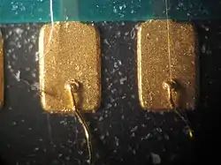
Contact pads or bond pads are designated surface areas of a printed circuit board (PCB) or die of an integrated circuit. Possibilities to contact to pads include soldering, wirebonding, flip chip mounting, or probe needles.

Gold wire ball-bonded to a gold contact pad
Further reading
- Jing Li, Evaluation and Improvement of the Robustness of a PCB Pad in a Lead-free Environment, ProQuest, 2007 ISBN 0-549-32110-1.
- Kraig Mitzner, Complete PCB Design Using OrCAD Capture and PCB Editor, Newnes, 2009 ISBN 0-08-094354-3.
- Deborah Lea, Fredirikus Jonck, Christopher Hunt, Solderability Measurements of PCB Pad Finishes and Geometries, National Physical Laboratory, 2001 OCLC 59500348.
This article is issued from Wikipedia. The text is licensed under Creative Commons - Attribution - Sharealike. Additional terms may apply for the media files.